The secret to PCB perfection (shhh, it’s inspection and testing)
The electronics business is made up of serious perfectionists whose basic assumption is that devices will perform flawlessly time after time. But perfection is hard to come by.
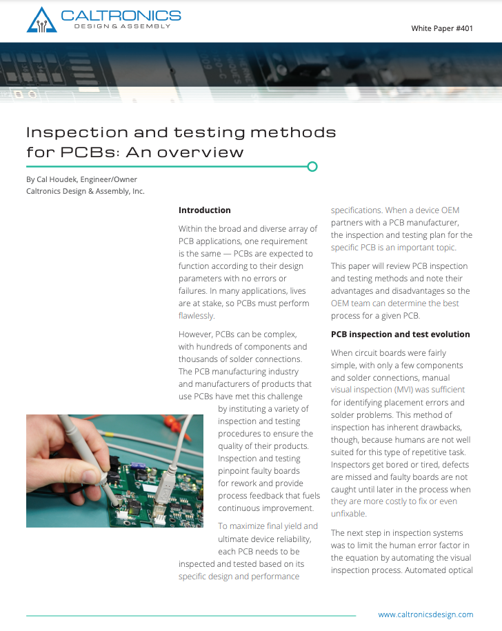
In the real world, a printed circuit board’s many components and solder joints must meet design specifications exactly for the PCB to function properly. To ensure perfection, inspection is a critical part of PCB fabrication.
What PCB inspection methodologies are there? Which ones will work best for your project? All you need to know is in our white paper.
When you’re selecting a PCB fabrication partner, look beyond design, manufacturing and assembly to consider PCB inspection. No inspection method is right for every PCB board, so look for a partner who has a range of equipment. Also, you’ll want your partner to have people with the technical know-how to help you develop and implement your PCB inspection plan.
PCB inspection at Caltronics
We offer a broad range of inspection capabilities—both 2D and 3D AOI as well as X-ray inspection. Caltronics’ comprehensive inspection program ensures that the pcb circuit boards and electronic assemblies we deliver meet the highest standards of quality. We can combine inspection methods so you get exactly the inspection services and PCB quality you need.
Learn more
Want to understand PCB inspection?