We Answer the 10 Common PCB Design and Assembly Questions Asked by Clients

We have compiled a list of 10 common questions we receive from clients before starting their design projects. We touch on topics including how our communication process works, our type of engineering services, how the project’s cost and timeline are determined, how we source materials, and much more. This list provides a baseline on how Caltronics operates but we encourage you to get in touch if you have further questions!
1. Who will I be communicating with during my project with Caltonics?
From design and circuit board manufacturing to using our PCB prototyping services, communication is a critical component to the success of a client’s project. Our team excels at both internal and external communication to ensure each member is knowledgable of the project and the client feels confident with the process. Therefore, we have a designated project manager that guides the project to guarantee the prototypes are properly designed and delivered both on time and on budget.
While the project manager, the lead designer, is the main point of communication, there are situations where the client will communicate directly with one of our specialized designers. This streamlines communication so that information is accurately delivered to increase the productivity of the project.
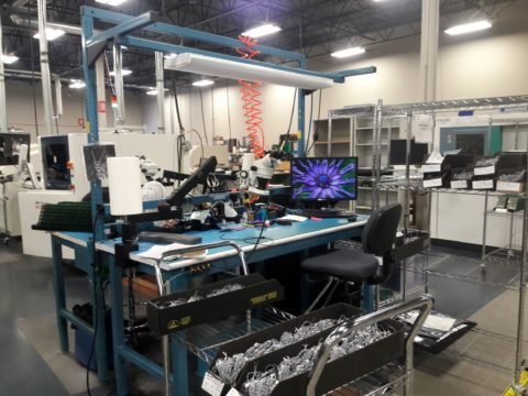
2. Who designs my project at Caltronics?
Caltronics has a team of design engineers with diverse specialties from embedded systems, Bluetooth and wireless communication, PCB layout software, and much more. The team’s wide range of expertise and extensive experience provides an authoritative perspective at each touchpoint of the project’s production.
3. What type of engineering services do Caltronics provide?
Our services include electrical, mechanical, and software engineering. Caltronics Design and Assembly is dedicated to developing an idea, and our innovative and comprehensive solutions reflect that mission. From circuit board design to PCB layout software, our engineering services address the needs for your PCB assembly and electronic design and manufacturing project.
4. How is the project cost determined?
The cost greatly depends on the type and scope of a project although there are two primary ways a budget is formulated.
First, if we are doing design for test (DFT) with a client, we provide a design scope requirements document that outlines how the process will be implemented. This provides a comprehensive review of how the design project will be achieved in order to define the quote for the project.
Second, if the project incorporates designing with the intent to be built for production, as compared to the first article or short prototype run, the production budget can be determined when the design is finalized and therefore the components are defined.
In addition to the design outline, the project’s timeline influences the budget. When a rapid production is required it subsequently increases the project cost. The next question addresses a project’s timeline considerations.
5. What is the typical project timeline?
A project’s timeline relies on the complexity of the printed circuit board, the availability of necessary parts, the client’s project budget, and Caltronics’ current workload. Delivery times for a design project typically vary from 12 weeks to 2 weeks, depending on the complexity of the design.
While we are capable of accelerated projects to comply with your company’s needs, we strive to keep the process at a practical speed to ensure each step of a project has been thoroughly addressed and vetted.
6. What is the turnkey process?
The turnkey PCB assembly process is broken down into five main steps and questions:
The client provides Caltronics with their Gerbers design files, or we provide the files if we have done the design.
Caltronics imports the bill of materials (BOM) or the comprehensive list of the parts needed for the project, how and where to acquire the material, and any instructions for assembly.
Determine if the project needs to be RoHS (Restriction of Certain Hazardous Substances) PCB compliant (lead-free) or a lead solder project. We set up the assembly process to meet those requirements.
Determine if the project needs to be ITAR (International Traffic in Arms Regulation) compliant and process accordingly.
Determine if the project requires PCB conformal coating.

7. What software can I use for my project with Caltronics?
Caltronics primarily uses SolidWorks and Altium Designer for design projects, although we have the capacity to import other design packages into our software.
8. What specific standards do Caltronics meet?
Caltronics is audited annually for ISO 9001:2015 standards confirming our ability to provide consistent products and services that satisfy the client and regulatory requirements. In addition, Caltronics is ITAR registered so we can conduct business with government contractors to provide space and defense industry parts.

9. How does Caltronics source their materials?
Caltronics Design and Assembly is a full-service shop from the initial design to the final assembly in order to ensure each step is efficiently designed, developed, and tested. We source materials from a broad range of suppliers to meet each project’s unique and specific needs.
For example, we have sourced specialized materials to meet the clients’ need for industrial-strength components that can withstand the heat or cold, low-cost options for simply electronics that require only basic functionality, domestically sourced or internationally sourced material, etc.
10. Why is the Caltronic inspection process different from others?
Caltronics uses a 3D automated inspector, the MIRTEC MV-6 automated optical inspection (AOI) machine, that significantly enhances our visual inspection process to ensure each PCB is optimally designed and manufactured.
We use a high-resolution X-Ray inspection machine to examine parts with solder joints under the components. We use and Yxlon Cheetah X-Ray machine.
While competitors often perform manual inspections, our process can detect and identify components that are not visible to the human eye. To learn more about our circuit board inspection equipment, please click here.

To Learn More Contact Caltronics
We’re always improving our machines to help create a solution quicker, faster, and less expensive for you to take to market. If you’re looking to design or manufacture an electronic product we can help. We have the tools and talent to build and assemble your next project.
Contact us or give us a call at 651.462.1440 today to get started!